Absolics Breaks Ground on Planned $600 Million Manufacturing Site in Georgia for Breakthrough Semiconductor Material
Facility will create more than 400 skilled jobs, strengthen the U.S. semiconductor supply chain
Increases total investment plans to more than $600 million
Material developed with Georgia Tech to support next-gen, high-performance computing
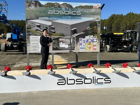
Absolics, Inc., a subsidiary of SKC Co. Ltd., broke ground today on a planned $600 million investment in Covington, Ga., for a new manufacturing facility that will supply advanced materials to the U.S. semiconductor industry.
The investment will create more than 400 high-skilled jobs in Georgia and help strengthen the U.S. semiconductor supply chain by manufacturing a new material that supports next-generation computing systems.
 are Consulate General of the Republic of Korea Yoonjoo Park, Director, 3D Systems Packaging Research Center (PRC) at the Georgia Institute of Technology Dr. Madhavan Swaminathan, SKC CEO Won Cheol Park, Georgia Department of Economic Development Commissioner Pat Wilson, Senator Jon Ossoff, Absolics CEO Jun Oh, Mayor of Covington, Steve Horton, and Newton County Chairman Marcello Banes.")


Absolics’ Georgia site will make a glass substrate – a thin layer of glass on which processing and memory chips can be mounted together to create the brains of a computing system. The material reduces the space required for a multi-chip package, allowing more chips to be packed into a single device.
See related articles: Historic Step: All Fifty States Plus D.C. and Puerto Rico Greenlit to Move EV Charging Networks Forward, Covering 75,000 Miles of Highway, Mercedes-Benz and Microsoft Collaborate to Boost Efficiency, Resilience and Sustainability in Car Production, Samsung Electronics To Invest Over $5 Billion As It Targets Net Zero By 2050
The glass substrate is considered a breakthrough because it can significantly increase the performance and energy efficiency of chipsets. SKC and Absolics originally developed the technology as part of a research consortium with the Georgia Institute of Technology. Absolics is expected to be the first in the world to mass produce the material.
The planned investment announced at today’s groundbreaking, attended by officials including Senator Jon Ossoff and Georgia Economic Development Commissioner Pat Wilson, represents an increase from the $473 million originally announced in October 2021. SKC and Absolics raised projections for the investment based on the need for more advanced manufacturing equipment to meet anticipated demand.
“Absolics will be an integral part of the semiconductor ecosystem in the U.S.,” said Dr. Woncheol Park, President and Chief Executive Officer of SKC. “We are pleased to build a factory and create hundreds of jobs that will have a positive impact on the city of Covington and the State of Georgia.”
“I am working every day to bring jobs and business to the State of Georgia,” said Senator Ossoff. “This new plant will create Georgia jobs, support U.S. national security, and bring more advanced manufacturing to our state.”
“The development of Absolics is an exciting opportunity to grow the semiconductor industry in Georgia and the entire United States – a need that is growing daily as we plan for an increasingly electrified future,” said Georgia Department of Economic Development Commissioner Pat Wilson. “Located at SKC’s existing campus in Covington, this new venture came about through research conducted at Georgia Tech, and it is the perfect example of how the State of Georgia is participating in the innovative solutions of the future. As we continue to build on the long-term relationship between the State of Georgia and Korea, and our shared success with SK Group in particular, we thank SKC for their commitment to our partnership. Congratulations to everyone involved with this project!”
Created to drive semiconductor innovations
Absolics was created last year by SKC, a majority owner of the new business. SKC is an operating company of SK Group, South Korea’s second-largest conglomerate with global companies in clean energy, semiconductors and life sciences.
Absolics plans to build the Georgia facility in two phases. The first phase, planned for completion by the end of 2023, will be a $240 million investment expected to create 140 jobs and focus on small-volume manufacturing. Mass production in this facility is expected to start in the second quarter of 2024. The second phase is expected to be an additional $360 million investment that creates another 270 jobs and ramps up to high-volume manufacturing. This phase is anticipated to be completed over the next 3-5 years.
Material enables more chips in less space
Absolics’ inaugural product will be a thin piece of glass, approximately 3-by-3 inches, used to package different semiconductor components together. Processing, memory and logic chips can be mounted next to each other on the glass to create the core of a computing system.
The standard today is to place these chips on a thin layer of silicon imposer that sits on top of a plastic substrate. The new glass material replaces both layers, simplifying the manufacturing process and reducing the thickness of the package by almost half. Certain components, such as multi-layer ceramic capacitors (MLCC), can be embedded in the glass substrate, freeing more space on the surface for chips.
The packaging component of the semiconductor industry is becoming more important as companies try to reach new levels of performance for their computing devices. Absolics’ product allows larger processors and up to four times more chips to be mounted in the same space.
The energy efficiency of the glass substrate also reduces overall power consumption by up to 50 percent, driving down costs and environmental impact, especially when applied at scale in large data centers.
Absolics expects the first phase to have an annual production capacity of 12,000 m2 with the second phase ramping up to annual production capacity of 72,000 m2.
Part of SK Group’s Broader U.S. Investments
The SKC investment and Absolics facility is part of a broader commitment by SK Group to increase its investments and assets in the U.S. to more than $50 billion by the end of 2025. The investments are intended to support industries critical to the global economy with a focus on clean energy, semiconductors and life sciences.
Earlier this year, SK Siltron CSS, a semiconductor wafer manufacturer, opened a new facility in Michigan as part of a $300 million investment to increase manufacturing capacity for semiconductor wafers that can be used in components for electric vehicles. SK On, one of world’s top makers of EV batteries, is investing $2.6 billion in a site in Commerce, Ga., to make batteries for electric vehicles.
Source: SKC Co. Ltd.